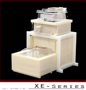
The use semiconductor materials such as silicon in the industry has become more and more popular today, particularly in the production of InGaN-based light-emitting diode. InGan or Indium Gallium Nitride is the light emitting layer you see in modern blue and green LEDs, often grown on a transparent substrate like sapphire. The high heat capacity and low sensitivity to ionizing radiation are ideal characteristics for solar photovoltaic devices, particularly useful for arrays of satellites.
With the help of wet etching process, particularly the al2o3 wet process (aka sapphire wet etching), numerous patterning features are produced on patterned sapphire substrates, paving the way for mass production aimed at filling a high-value gap in the rapidly growing global LED market as more and more industries recognize the value of this type of material for lighting and illumination – uses where energy efficiency, low production cost, and environment-friendly process are very important for sustainable energy platform.
The Sapphire etching demand for semiconductor production
In the market research report published by Strategies Unlimited, the demand for LED products, particularly the high-brightness LED grew from USD 5.6 bn in 2009 to USD 10.8 bn in 2010. The study also revealed that this demand could grow about USD 18.9 bn by 2015. This trend is considered to be one of the factors why the demand for sapphire etching has grown significantly.
Wet process advantages
There are two major advantages of wet process particularly the al2o3 wet etching process. First, it is extremely fast and (second) it is a lot cheaper than dry etching. Furthermore, wet process is far more advantageous when it comes to scalability or the ability to handle a growing amount of in a capable manner.
The wet etching process
During high-temperature wet etching, it involves the following processes:
-
Gallium nitride or indium gallium nitride coated wafers are put in a tank that contains a mixture of etching and buffering agents.
-
A silicon dioxide mask is spun onto the sapphire substrate through a plasma-enhanced vapor process
-
Lithography is utilized to expose the desired pattern.
-
Specific temperatures are then applied to the mixture – ideally between 260 and 300 degrees Celsius.
The current trend in wet etching and semiconductor industry is expected to grow more in the coming years. Along the way, we’ll probably see more innovations that that can make the process more improved.

